It's a 32-bit processor:
But memory is byte addressable (every byte gets sent to a separate address, 4 bytes at 4 separate addresses).
Words are stored in addresses divisible by 4. For example:
t0 = 0(t0) → Address 0x2cnext word: 4(t0) → Address 0x30next word: 8(t0) → Address 0x34next word: c(t0) → Address 0x38Initializing memory with values: Assembler directives begin with a dot (.). Some
examples:
.word 10 → Puts a word size of 10 in the memory. Word is 4 bytes..byte 50 → Puts 50 in the next byte..hword 20 (half word) → Puts 20 in the next 2 bytes.If we didn't have labels, we would have to figure out what the numbers for the actual addresses are (that change every time we insert/delete something in the program)
| Instruction | Explanation |
|---|---|
li a0, 10 |
addi a0, zero, 10 (also: a0 = 0 + 10) |
li a0, 0x12345678 |
lui a0, 0x12345 (also: Load upper 20 bits (0x12345000))addi a0, a0, 0x678 (also: Add lower 12 bits (0x00000678))
|
.global _start
_start:
    # Load immediate values into registers
    li a0, 10        # a0 = 10
    li a1, 20        # a1 = 20

    # Load values from memory
    la a2, var1      # Load address of var1 into a2
    lw a3, 0(a2)     # Load value at var1 into a3 (a3 = 10)

    la a2, var2      # Load address of var2 into a2
    lw a4, 0(a2)     # Load value at var2 into a4 (a4 = 20)

    # Arithmetic operations
    add a5, a0, a1   #a5 = a0 + a1  (10 + 20 = 30)
    sub a6, a1, a0   # a6 = a1 - a0  (20 - 10 = 10)

    # Logical operations
    and a7, a0, a1   # a7 = a0 & a1  (bitwise AND)
    or t0, a0, a1    # t0 = a0 | a1  (bitwise OR)
    xor t1, a0, a1   # t1 = a0 ^ a1  (bitwise XOR)

    # Shift operations
    slli t2, a0, 2   # t2 = a0 << 2  (Shift left by 2 bits) 1111 -> 1100
    srli t3, a0, 2   # t3 = a0 >> 2  (Logical shift right) 1111 -> 0011
    srai t4, a0, 2   # t4 = a0 >> 2  (Arithmetic shift right) can shift negative numbers (copies most significant bit)

    # Comparison
    slt t5, a0, a1   # t5 = (a0 < a1) ? 1 : 0  (10 < 20 → t5 = 1)
    sltu t6, a1, a0  # t6 = (a1 < a0 unsigned) ? 1 : 0  (unsigned comparison)

    # Branching
    beq a0, a1, equal_case  # If a0 == a1, jump to equal_case
    bne a0, a1, not_equal   # If a0 != a1, jump to not_equal
    blt a0, a1, less_case   # If a0 < a1, jump to less_case
    bge a1, a0, greater_case # If a1 >= a0, jump to greater_case

equal_case:
    li t6, 100   # t6 = 100 (this won't execute)
    j exit

not_equal:
    li t6, 200   # t6 = 200
    j exit

less_case:
    li t6, 300   # t6 = 300
    j exit

greater_case:
    li t6, 400   # t6 = 400
    j exit

    # Jump and Link (Function Call Simulation)
call_function:
    jal function   # Jump to function and save return address in ra
    j exit

function:
    addi sp, sp, -4   # Allocate stack space
    sw ra, 0(sp)      # Store return address
    li a0, 42         # Set return value
    lw ra, 0(sp)      # Restore return address
    addi sp, sp, 4    # Deallocate stack space
    ret               # Return to caller

exit:
    # Atomic operations (only in RV32A)
    la a0, var1       # Load address of var1
    li a1, 5
    amoadd.w a2, a1, (a0)  # var1 += 5 (Atomic addition)

    # Store result to memory
    sw a5, 0(a2)      # Store a5 into var1

    # System call to exit
    li a7, 10         # System call ID for exit

meByte: .byte 0x55
.skip 3               # Jump ahead 3 bytes (without this, the code will be misaligned)
.align 4              # Goes to the next address divisible by 4 (use only one of these)
meWord: .word 0x88776622
.data
var1:   .word 10    # Define a memory location var1 with value 10
var2:   .word 20    # Define a memory location var2 with value 20
Program counter points to the next instruction to be executed.
Different ways to call a function
call my_function # ra <- pc
my_function:
Jump (pseudo for
jal x0, my_function)
j my_function # ra <- pc
my_function:
main:
jal ra, func  # Jump to func, save return address in ra
# Execution resumes here after func returns
func:
# Do something
ret  # Equivalent to `jalr x0, ra, 0`
Return
my_function:
ret # pc <- ra
Stacks grow downwards (from address 100 -> 1). Our stacks in this course start at 0x20000 (the first address is actually never used by the stack it is free to be used by anything else in the program).
Little endian: low order byte goes on low address.
# Initialize stack pointer
la sp, 0x20000
li t0, 0x12345678
# Push
addi sp, sp, -4
sw t0, (sp)
# Pop
lw t1, (sp)     # t1 <- sp
addi sp, sp, 4  # sp <- sp + 4
# Now this is removed from the stack but is popped in t1
| Address | Data/Byte Address |
|---|---|
| 0x1FFFC | 0x78 |
| 0x1FFFD | 0xF6 |
| 0x1FFFE | 0x34 |
| 0x1FFFF | 0x12 |
| 0x20000 |
To store multiple return addresses. Used when we need nested functions, recursive function calls, or generally want to avoid overwriting ra.
addi sp, sp, -4
sw ra, (sp)      # Push ra onto the stack
                    # Order is important, can't do sw then addi because what if interrupt

.
.
call another_subroutine
.
.

lw ra, (sp)      # Pop ra from the stack
addi sp, sp, 4

ret
a0 ... a7: argument register
t0 ... t6: temporary
s0 ... s11: save registers
LUTs (look up table) are used as small memory elements inside logic blocks to implement combinational logic functions.
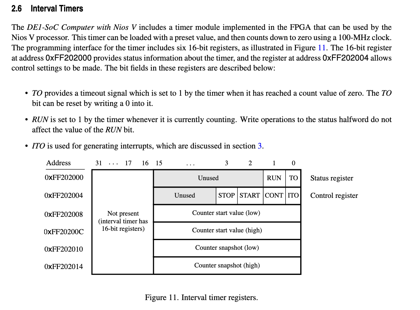
| Address | Registers | What's in it |
|---|---|---|
| 0xFF202000 | Status Register | _ _ _ _ _ _ _ _ _ _ _ _ _ _ _ _ _ _ _ _ _ _ _ _ _ _ _ _ _ _ RUN TO (last 2 bits used, others unused) (read/load) |
| 0xFF202004 | Control Register | _ _ _ _ _ _ _ _ _ _ _ _ _ _ _ _ _ _ _ _ _ _ _ _ _ _ _ _ STOP START CONT ITO (interrupt) (write/store) |
| 0xFF202008 | Counter Start Value Part 1 | _ _ _ _ _ _ _ _ _ _ _ _ _ _ _ _ 0 0 0 0 0 0 0 0 0 0 0 0 0 0 0 0 (lower 16 bits of Counter Start Value) |
| 0xFF20200c | Counter Start Value Part 2 | _ _ _ _ _ _ _ _ _ _ _ _ _ _ _ _ 0 0 0 0 0 0 0 0 0 0 0 0 0 0 0 0 (upper 16 bits of Counter Start Value) |
| 0xFF202010 | Current Value of Counter Part 1 | _ _ _ _ _ _ _ _ _ _ _ _ _ _ _ _ 0 0 0 0 0 0 0 0 0 0 0 0 0 0 0 0 (lower 16 bits of Counter Snapshot) |
| 0xFF202014 | Current Value of Counter Part 2 | _ _ _ _ _ _ _ _ _ _ _ _ _ _ _ _ 0 0 0 0 0 0 0 0 0 0 0 0 0 0 0 0 (upper 16 bits of Counter Snapshot) |
.equ TIMER_BASE, 0xFF202000
.equ COUNTER_DELAY, 100000000
.equ LEDs, 0xFF200000

# Set up counter
_start:
la t5, TIMER_BASE
sw zero, 0(t5)              # Clearing the TO bit in status register
li t0, COUNTER_DELAY        # Counter Start Register
srli t1, t0, 16             # Shift the upper 16 bits of the delay into the lower 16 bits of t1
sw t1, 0xc(t5)              # Put that into counter start high register
# Set up control bit (turn on CONT and START)
li t0, 0b0110
sw t0, 4(t5)
la t6, LEDs
li t2, 1                    # Next of LED0
tloop: sw t2, (t6)          # Set LED0
        xori t2, t2, 1       # Invert bit 0 of t2
ploop: lw t0, (t5)          # Load "Timer Status Register"
        andi t0, t0, 1       # Isolate bit 0 -> t0
        beqz t0, ploop
        sw zero, (t5)        # Reset t0
        j tloop
signal ___---___ -> edge capture ______---. Basically captures the negative edge and stores it so we know the xyz signal condition has happened.
Writing 1 in an edge capture register bit erases it! Writing 0 keeps it as is
If we do edge capture with keys for example: Memory address 0xFF200050
| Address | Registers | What's in it |
|---|---|---|
| 0xFF200050 | Data Register | _ _ _ _ _ _ _ _ _ _ _ _ _ _ _ _ _ _ _ _ _ _ _ _ _ _ _ _ 0 0 0 0 (last 4 bits used, others unused) |
| 0xFF200054 | Direction Register | ignore |
| 0xFF200058 | Interrupt Mask Register | _ _ _ _ _ _ _ _ _ _ _ _ _ _ _ _ _ _ _ _ _ _ _ _ _ _ _ _ 0 0 0 0 (write 1 to mask the bit) |
| 0xFF20005c | Edge Capture Register | _ _ _ _ _ _ _ _ _ _ _ _ _ _ _ _ _ _ _ _ _ _ _ _ _ _ _ _ 0 0 0 0 (last 4 bits used, others unused) |
la a1, edgecapture
lw s0, (a1)
andi s1, s0, 0b1111 # (isolate 4 bits of edge capture register)
li s1, 0b1111 # 1 erases the edge capture register to 0
sw s1, (a1)
Edge capture is how we actually interrupt something - write a 1 in bit 0 of interrupt mask register means whenever there's a 1 in the bit 0 of edge capture register, have that requests an interrupt. (Must turn off the edge capture bit - usually by user)
.equ KEY_BASE, 0xFF200050
la t0, KEY_BASE

# Polling Loop
poll: lw t1, (t0)
andi t1, t1, 0010   # bit mask
beqz t1, poll

# Arrive here when button is pressed
Make sure to pay attention to Lecture 14 (or whichever is Applying Interrupts to an Example I/O (KEYS for 2025))
Imagine it as adding another bus that is a "Interrupt Request Handler" -> Once an interrupt is caused then an action is taken, no continous mindless polling. Returns to the same instruction after working on the interrupt coming back to the same instruction as if nothing has happened (eg. no registers overwritten).
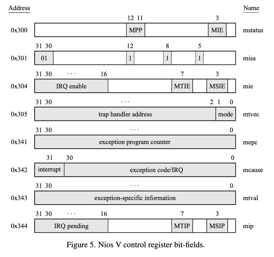
Registers:
csrw mstatus, zerola t0, interrupt_handler_func
csrw mtvec, t0li t0, 0x40000 (IRQ18)
csrs mie, t0la t0, 0xFF200050
li t1, 0b1111 (if turning on a specific key, change this number)
sw t1, 8(t0)li t0, 0b1000
csrw mstatus, t0Interrupts allow a processor to temporarily pause its current execution to handle external events, ensuring synchronization with peripherals.
| Processor | Communication | I/O |
|---|---|---|
| FSM | IRQ18 | KEYS |
| IRQ16 | Interval Timer |
In the diagram above, the things on the left are NOT addresses.
C is compiled to Assembly which is coded into numbers and space in memory that is coded into binary
# This is the program in assembly
.global _start
.equ LEDs, 0xFF200000
.equ SW, 0xFF200040

_start:
    la t0, LEDs
    la t1, SW
loop:
    lw t2, (t1)
    sw t2, (t0)
    j loop
// This is the same program in C

int main (void){
    volatile int *LED_ptr = 0xFF200000;
    volatile int *SW_ptr = 0xFF200040;
    int value;

    while (1){
        value = *SW_ptr;
        *LED_ptr = value;
    }
}
Example: Guitar (Audio as sound pressure waves)
Person -> Microphone -> Amplifier -> ADC -> INPUT FIFO (does: store (not load)) -> 2<3<4<3<2<1 -> Computer -> OUTPUT FIFO -> DAC (output V)-> Amplifier -> Speaker
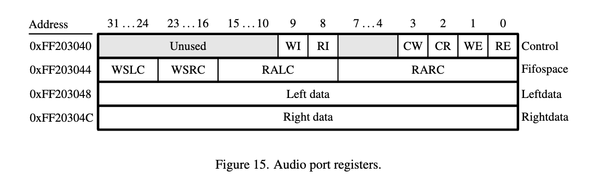
Memory-mapped input-output, we will be able to access registers to some address, same as previously discussed memory-mapped I/O. But this one is more complex. Processor, Memory, Audio -> cannot connect wi the specific memory-mapped registers that connect to input/output FIFOs fo the audio unit. 2 channels: 2 output FIFOs, 2 input FIFOs. Reading something takes it OUT of the FIFO.
            32 bits memory address:
            0xFF203040: 9: WI, 8: RI, 3: CW, 2: CR, 1: WE, 0: RE control/status
            0xFF203044: 31-24: WSLC, 23-16: WSRC, 15-8: RALC, 7-0: RARC fifospace
            0xFF203048: 23-0: Left Data
            0xFF20304c: 23-0: Right Data
fun fact: this is where real hardware > cpulator (part2, 4 of lab 6)
for the project: a lot of samples, need the list of samples
int samples[] = {so, many, samples, so, many, samples, x20000}Need to make sure that the sound is correctly sampled.
        #define AUDIO_BASE 0xFF203040

        int main (void){
            volatile int* audio_ptr = (int*) AUDIO_BASE;
            int left, right, fifospace;
            while(1){
                fifospace = *(audio_ptr + 1); //because pointer arithmetic: integer = 32 bits, next 1 is next 4 bits so 1 and not 4
            }
            if ((fifospace &0x000000FF)>0){ //right input fifo is not empty
                //load the 2 input channels if there is something there
                left = *(audio_ptr + 2); //same as lw t0, 8(t1)
                right = *(audio_ptr + 3);
                *(audio_ptr + 2) = left;
                *(audio_ptr + 3) = right;
            }
        }
To accurately represent a signal with a maximum frequency of x, you must sample it at a rate of at least 2x. This ensures the signal can be perfectly reconstructed.
Resolution: 320px (horizontal) x 240px (vertical)
through these memory mapped registers:
| Address | Register | Notes |
|---|---|---|
| 0xFF203020 | Front buffer address | default address 0x08000000, cannot change the address in this register (only changes with a swap) |
| 0xFF203024 | Back buffer address | |
| 0xFF203028 | ||
| 0xFF20302c | Status Register |
Function to wait for vsync
        void wait_for_vsync(){
            volatile int* fbuf = (int*) 0xFF203020; //base of VGA controller
            int status;
            *fbuf = 1; //start swap cycle per 1
            status = *(fbuf + 3); //read status register
            while ((status & 0x01)!=0){
                status = *(fbuf + 3);
            }
        }

// my first cuda program __global__ void arradd(float *a, float fade, int N){ int i = blockIdx.x * blockDim.x + threadIdx.x; if (i < N) a[i] *= fade; } int main(){ float *a, *d_a; int N = 1000000; a = (float*)malloc(N*sizeof(float)); cudaMalloc(&d_a, N*sizeof(float)); cudaMemcpy(d_a, a, N*sizeof(float), cudaMemcpyHostToDevice); } arradd<<<1, 1024>>>(d_a, 0.5f, N);Citations
[1] Github.com, 2025. https://github.com/fpgacademy/Tutorials/releases/download/v21.1/Nios_V_Intro.pdf (accessed Mar. 09, 2025).[2] "DE1-SoC Computer System with Nios ® V.” Accessed: Mar. 09, 2025. [Online]. Available: https://fpgacademy.org/Downloads/DE1-SoC_Computer_NiosV.pdf